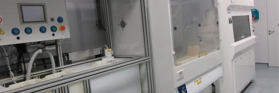
Part of the nanofabrication cleanrooms
We offer a range of equipment for processing Cu in dedicated areas of our Integrated Photonics Cleanroom (IPC). Samples or wafers containing Cu are deposited, lithographically defined, etched, polished, and electroplated. This is supported by a materials policy that is more relaxed than typical CMOS fabrication facility.
We assist with BEOL processing or preparation for bonding, using diced samples up to 200 millimetres (mm) SEMI standard wafers.
- planarisation of Cu interconnect layers
- fabrication of Cu re-distribution layers (RDLs)
- electroplating and planarisation of through wafer vias
- seeding and electroplating of Cu films
- die stacking and 3D packaging
- die to wafer bonding

Processes and equipment
Deposition
- Edwards electron beam evaporators
Lithography
- EVG620TB for up to 200mm front side alignment, 150mm backside
Chemical Mechanical polishing (CMP)
- dedicated Logitech CM62 Orbis CMP tool for Cu processing
Wet etch
- dedicated wet bench for Cu etch and substrate cleaning
Electroplating
- heated electroplating tanks suitable for 100, 150, or 200mm wafers
Contact us
For more information or to book the facilities, get in touch: zepler.cleanrooms@soton.ac.uk
