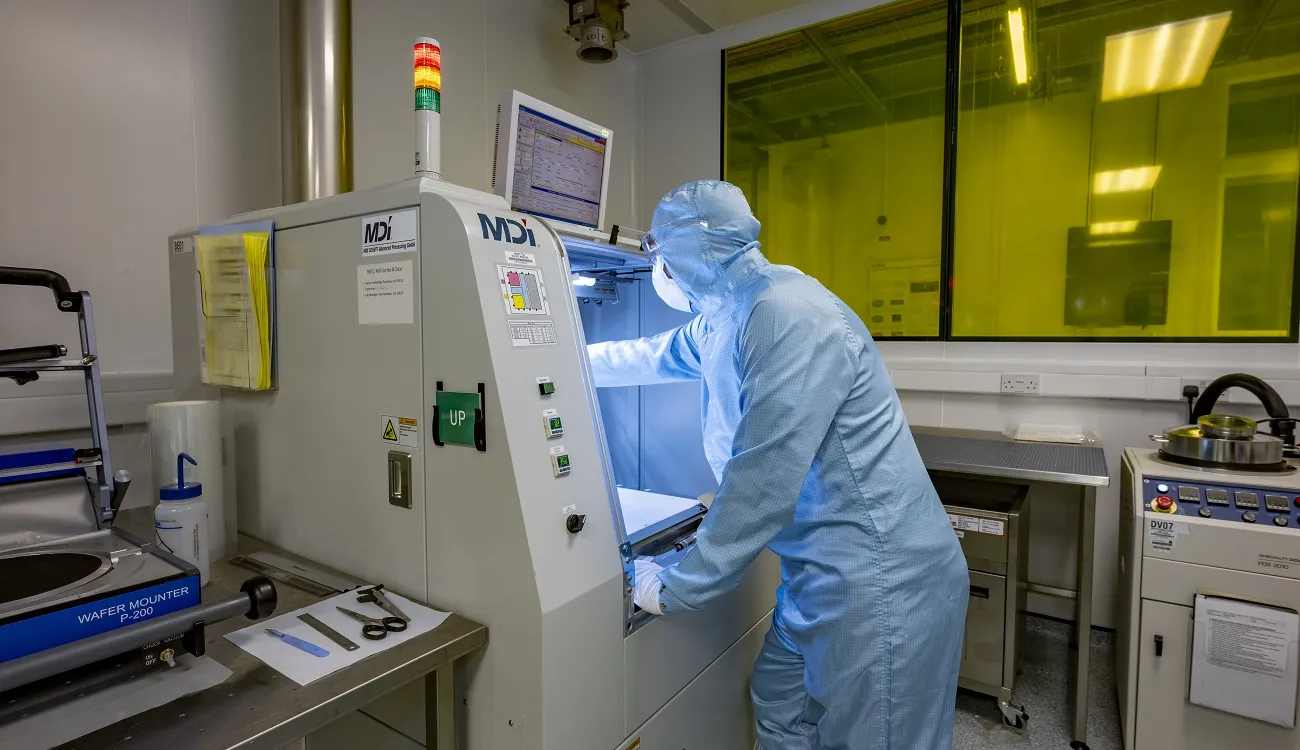
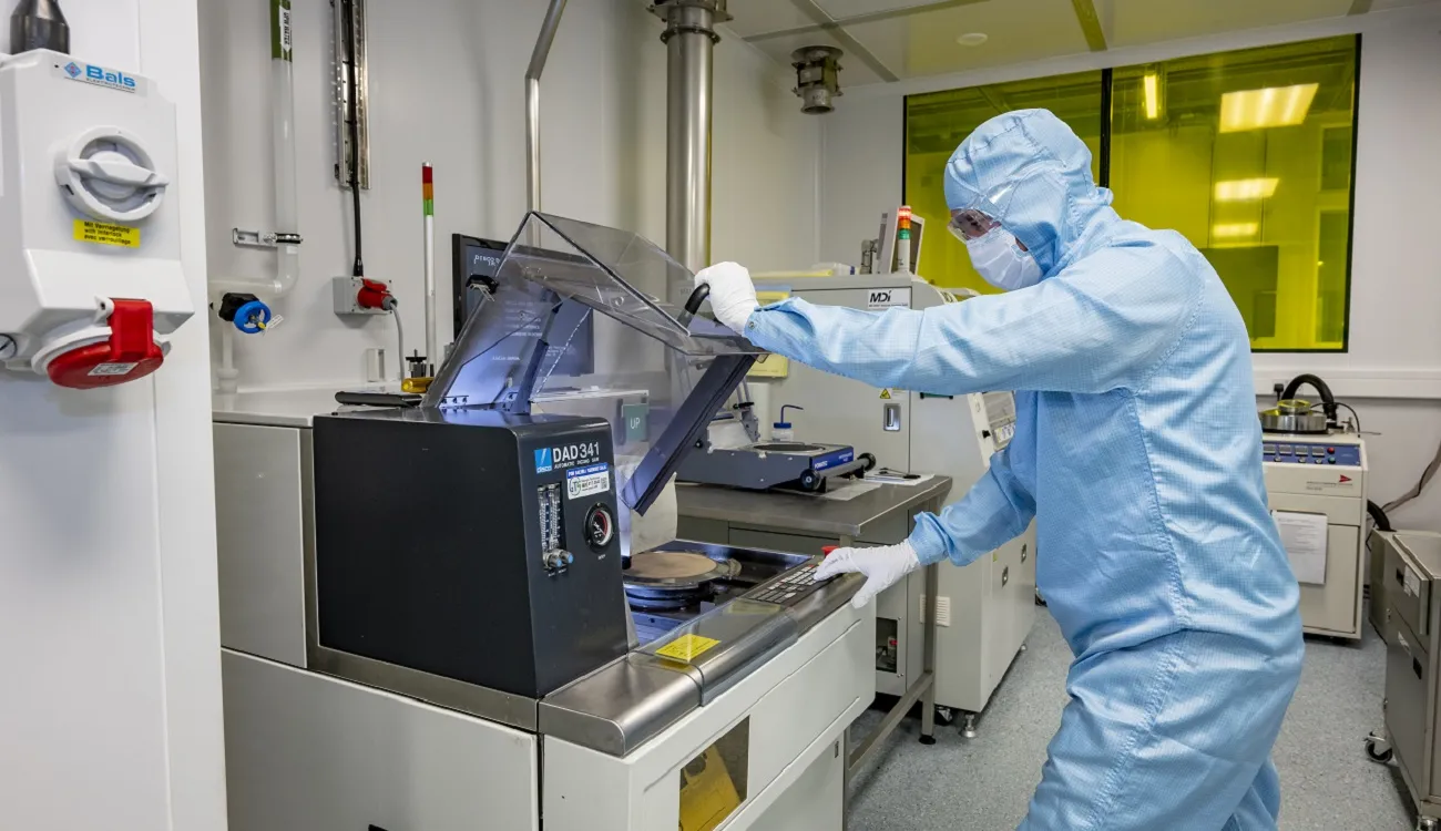
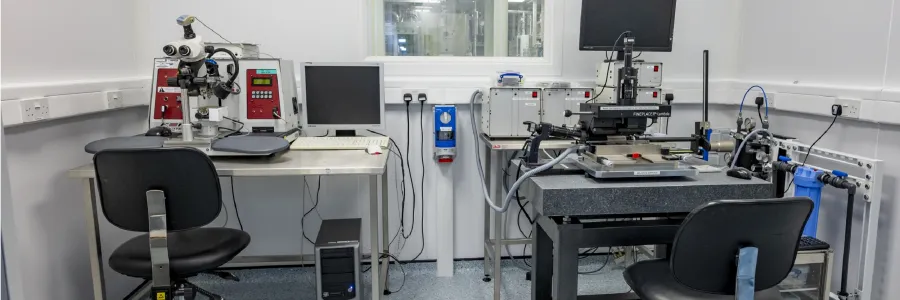
Part of the nanofabrication cleanrooms
The nanofabrication cleanrooms have a range of finishing technologies to enable post-fabrication packaging. We offer automated dicing up to 200 millimetres (mm), and semi-automated scribing of substrates up to 400mm. We create device connections via manual wirebonding, manual flip chip bonding, or automated flip chip die bonding.
We can also prototype novel processes. These include:
- wafer-wafer polymer/glue bonding
- microfluidic system encapsulation
- flip chip bonding for heterogenous integration. For example, III-V components onto silicon or dielectric waveguide substrates

Processes and equipment
Scribing and dicing
- dicing saw for silicon (Si), germanium (Ge), III-V substrate sizes from small samples up to 200mm wafers, position accuracy 0.5 micrometres (μm)
- Mitsuboshi Diamond Industrial scriber for Si, silicon dioxide (SiO2), and sapphire substrates up to 400mm per side
Manual bonding
- manual flip chip bonding, 0.5μm accuracy, 1-400 newtons, up to 550°C
- manual wirebonder for gold and aluminium (Al, Au)
Automated bonding
- ASMPT Amicra nano die bonder for automated pick and place flip chip heterogeneous integration applications. Positioning capability 0.3μm to 1 standard deviation

Contact us
For more information or to book the facilities, get in touch: zepler.cleanrooms@soton.ac.uk
