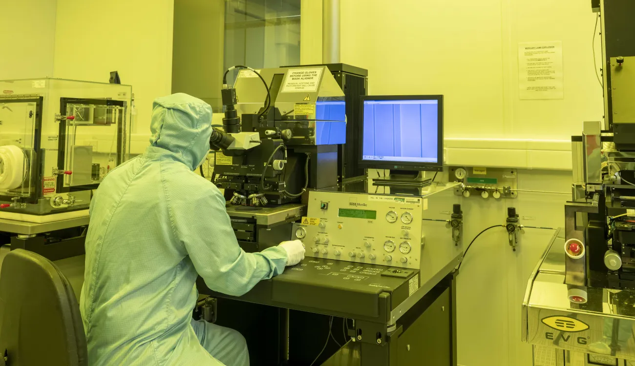
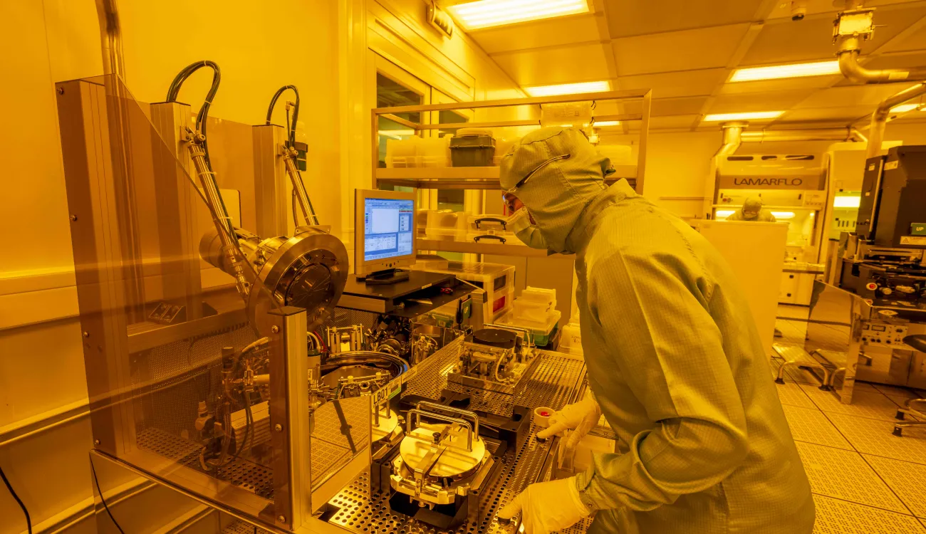
Part of the nanofabrication cleanrooms
Lithography is the technique by which design patterns are transferred to a sensitive resist at multiple stages of the fabrication process.
Our lithography capability features leading Electron Beam Lithography (EBL), writing to 5 nanometres (nm) feature size. Unique to UK academic research we also have a Deep Ultraviolet (248nm) scanner for feature size down to 180nm.
We also provide traditional broadband UV photolithography using manual mask aligners, for feature size down to 1 micrometre (µm).
The mask aligners operate in contact or proximity modes. They handle a range of substrate sizes, from small pieces up to 200 millimetre (mm) wafers, in front and backside alignment modes. We can fit the aligners with optical filters to allow G/H/I line wavelength selection.
Alternative nanopatterning techniques such as microcontact printing and nano imprint lithography are also available.
Our wafer bonder can perform pre-bond alignment via a mask aligner. This achieves micron-scale bond alignment accuracy.
We offer a versatile capability for resist processing, including multiple spin, bake, and development lines.
We work with many types of resists including:
- positive and negative tone UV photoresists
- electron beam resists
- thick film photoresists up to 100µm
- SU-8 epoxy photoresists
- laminated epoxy and acrylic photosensitive materials
Advanced photolithography facilities
Processes and equipment
Spin and bake
- CEE Apogee modules for separated optical and electron beam resist spin and bake
Optical photolithography (Broadband/G/H/I Line compatible)
- EVG620 & Karl Suss MA6 Broadband contact aligners
- 200mm frontside alignment
- 200mm front to backside alignment, bonding alignment, UV nanoimprint processes. Minimum standard feature size 1µm
- optimised for positive, negative, and LoF resists, polymers (SU-8, bonding)
- substrate sizes up to 200mm (other chucks available to handle smaller substrates)

Wafer bonding
- EVG 520 capable of performing thermo-compression, Fusion, Anodic, Eutectic and Adhesive bonding
- process temperature up to 500°C
- contact force up to 20 kilonewtons
- substrate sizes from pieces to 150mm wafers
- compatible with EVG 620TB for pre-bond wafer alignment
Resist processing
- optimised processes for scanner, e-beam, and optical lithography applications
- established positive, negative, lift-off, and image reversal resist processes
- polymer and spin-on glass coatings for bonding, structural materials, microfluidics, and encapsulation
- thickness ranges from nm to > 100µm
- dedicated resist spinners
- 300°C maximum temperature hotplate for substrates up to 200mm
- dehydration and resist bake ovens
- mask cleaner and lift-off station
- O2 microwave plasma ashing
- dedicated wet resist strip stations

Contact us
For more information or to book the facilities, get in touch: zepler.cleanrooms@soton.ac.uk
