Magic - Simulation with HSpice
Magic designs may be simulated using either HSpice (analog simulation) or
Verilog (digital simulation).
This document describes the creation of HSpice files and the use of the
HSpice simulator.
File creation
Generate ".ext" files for your design
Generate ".spice" and ".sp" files for your toplevel cell
This creates
"<cellname>.spice"
a transistor level spice netlist of your magic design
(included automatically in "<cellname>.sp")
In the case of the loaded inverter circuit designed in the
magic hierarchy exercise,
the file should look like this:
* HSPICE file created from inv_ld.ext - technology: cmos05

.option scale=0.1u

m0 n2 out Vdd Vdd pmos0553 w=25 l=5
+ ad=143 pd=60 as=1980 ps=474
m1 n2 out GND GND nmos0553 w=11 l=5
+ ad=655 pd=258 as=0 ps=0
m2 n1 out Vdd Vdd pmos0553 w=25 l=5
+ ad=143 pd=60 as=0 ps=0
m3 n1 out GND GND nmos0553 w=11 l=5
+ ad=655 pd=258 as=0 ps=0
m4 out in Vdd Vdd pmos0553 w=25 l=5
+ ad=563 pd=208 as=0 ps=0
m5 out in GND GND nmos0553 w=11 l=5
+ ad=1550 pd=638 as=0 ps=0
C0 out GND 4.6fF

** hspice subcircuit dictionary
"<cellname>.sp"
a skeleton spice stimulus file for you to edit
In the case of the loaded inverter circuit designed in the
magic hierarchy exercise,
the file should look like this:
** HSPICE file for inv_ld
**   - generated by ext2sp v3.1

** Include netlist file for inv_ld
.include inv_ld.spice

** Default 3.3V Power Supply
Vsupply Vdd GND 3.3V

** Specify input signals here
** e.g. for inputs A and B
**   VA A GND PWL(0NS 0V  2NS 0V  2.25NS 3.3V  6NS 3.3V  6.25NS 0V)
**   VB B GND PWL(0NS 0V  4NS 0V  4.25NS 3.3V  8NS 3.3V  8.25NS 0V)

** Default Simulation - Type, Resolution & Duration
.TRAN 10PS 10NS

** Specify ouput signals to measure here
** e.g. rise and fall delays for output Y
**   .measure tran fall_delay TRIG v(Y) VAL='3.3*0.9' TD=0NS FALL=1
**   + TARG v(Y) VAL='3.3*0.1' TD=0NS FALL=1
**   .measure tran rise_delay TRIG v(Y) VAL='3.3*0.1' TD=0NS RISE=1
**   + TARG v(Y) VAL='3.3*0.9' TD=0NS RISE=1

** Save results for display
.OPTIONS POST

.END
- note that unless you use the "-f" option, the ".sp" file
will not be overwritten by subsequent uses of ext2sp on
the same cell.
Edit the stimulus information within the ".sp" file.
edit the "<cellname>.sp" using your favourite editor.
Power Supply
The default 3.3V power supply, Vsupply, between Vdd and GND should be
fine provided that you have labelled your design correctly.
Input Signals
You must add an input specification for each of your cell's inputs.
For digital cells it is usual to specify the inputs as Piece-Wise Linear
voltage sources referenced to the GND node. The example:
VA A GND PWL(0NS 0V 2NS 0V 2.25NS 3.3V 6NS 3.3V 6.25NS 0V)
describes a voltage source called VA (all voltage souces begin
with a V) between node A and GND.
Within the brackets there are a number (in this case 5) of time,
voltage pairs which fully describe voltage source.
The figure below shows the waveforms generated at nodes A and B
by the two example PWL statements:
VA A GND PWL(0NS 0V  2NS 0V  2.25NS 3.3V  6NS 3.3V  6.25NS 0V)
VB B GND PWL(0NS 0V  4NS 0V  4.25NS 3.3V  8NS 3.3V  8.25NS 0V)

In the case of the loaded inverter example we wish to describe a
voltage source on the node labelled in so we might include
the line:
Vin in GND PWL(0NS 0V 2NS 0V 2.25NS 3.3V 6NS 3.3V 6.25NS 0V)
which describes a voltage source called Vin between in and
GND with the same Piece-Wise Linear shape as the VA
example above.
Simulation Specification
The default simulation type is .TRAN, a transient analysis,
this is suitable for the investigation of simple digital circuits.
The simulation resolution defaults to 10ps. You may change this if
you wish.
The simulation duration defaults to 10ns. You should ensure that this
time is long enough to observe the response to the last change in the
inputs.
Measurement
Although measurements can easily be made from the waveforms once
the simulation is complete, inclusion of .measure commands
in the "<cellname>.sp" file provides an automated
method of measuring rise, fall and propagation delay times during
simulation.
In each case the command measures the time between a TRIGger
time and a TARGet time described in terms of the behaviour
of a signal.
The following measurement for the fall delay on
signal out, specifies that the trigger time is the first
time the out signal falls past the 3.3v×90% while
the target time is the first time the out signal falls
past the 3.3v×10%:
.measure tran fall_delay
+ TRIG v(out) VAL='3.3*0.9' TD=0NS FALL=1
+ TARG v(out) VAL='3.3*0.1' TD=0NS FALL=1

To measure a propagation delay, the threshold voltages will be set
at 3.3v×50% and the trigger will be taken from
a transition on the input signal:
.measure tran propagation_f
+ TRIG v(in) VAL='3.3*0.5' TD=0NS RISE=1
+ TARG v(out) VAL='3.3*0.5' TD=0NS FALL=1

For details on writing .measure commands see page 2-92 of the
Hspice Command Reference
manual.
At the end of this editing process the "inv_ld.sp" file for the
loaded inverter is only slightly changed:
** HSPICE file for inv_ld
**   - generated by ext2sp v3.1

** Include netlist file for inv_ld
.include inv_ld.spice

** Default 3.3V Power Supply
Vsupply Vdd GND 3.3V

** Specify input signals here
Vin in GND PWL(0NS 0V  2NS 0V  2.25NS 3.3V  6NS 3.3V  6.25NS 0V)

** Default Simulation - Type, Resolution & Duration
.TRAN 10PS 10NS

** Specify ouput signals to measure here
.measure tran fall_delay TRIG v(out) VAL='3.3*0.9' TD=0NS FALL=1
+ TARG v(out) VAL='3.3*0.1' TD=0NS FALL=1
.measure tran propagation_f TRIG v(in) VAL='3.3*0.5' TD=0NS RISE=1
+ TARG v(out) VAL='3.3*0.5' TD=0NS FALL=1
.measure tran rise_delay TRIG v(out) VAL='3.3*0.1' TD=0NS RISE=1
+ TARG v(out) VAL='3.3*0.9' TD=0NS RISE=1
.measure tran propagation_r TRIG v(in) VAL='3.3*0.5' TD=0NS FALL=1
+ TARG v(out) VAL='3.3*0.5' TD=0NS RISE=1

** Save results for display
.OPTIONS POST

.END
Simulation
Run the simulator
View the signal waveforms
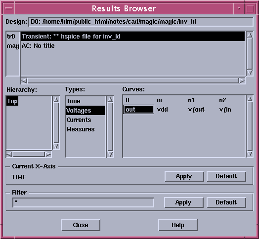
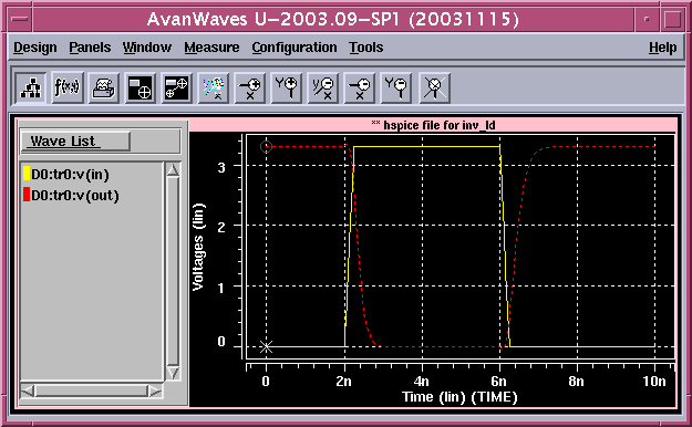
Using the Results Browser window, first select the Transient
analysis for the loaded inverter. Next select the in and
out signals for display by double clicking the left mouse
button over each of the signal names in turn.

The result should look like this:

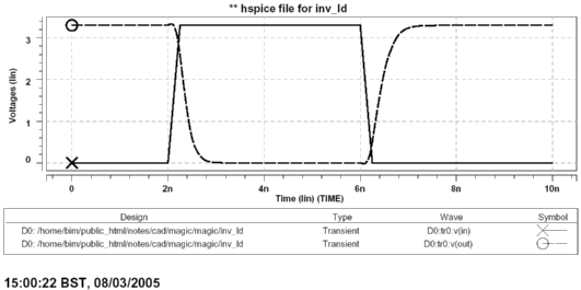
The AvanWaves (awaves) waveform viewer includes a facility
to print the waveforms via the Tools menu.
The resulting printouts are suitable for sticking in
your log book or including in a report (use the "print to
file" option and select "EPS" format to get a file suitable
for inclusion by most word processors):

AvanWaves also includes a facility to take measurements from
the waveforms displayed via the Measure menu.
For more details of this facility and of other features of
AvanWaves see the
AvanWaves User Guide.
View the results of the .measure commands
Results are given in scientific notation with no units
(e.g. propagation_f = 2.249e-10 ) so you will need to
convert them into picoseconds or nanoseconds before
presenting them in any report (e.g.
Propagation delay
from in↑ to out↓ is 0.22ns).
Remember to perform "sanity checking" on your numerical
results. If the value provided by the .measure command
doesn't make sense when you try to match it to the waveforms
then you've probably mis-specified either the TRIGger or the
TARGet.
Additional Documentation


