Magic - Simulation with HSpice
Magic designs may be simulated using either HSpice (analog simulation) or
Verilog (digital simulation).
This document describes the creation of HSpice files and the use of the
HSpice simulator.
File creation
Generate ".ext" files for your design
Generate ".spice" and ".sp" files for your toplevel cell
This creates
"<cellname>.spice"
a transistor level spice netlist of your magic design
(included automatically in "<cellname>.sp")
In the case of the loaded inverter circuit designed in the
magic hierarchy exercise,
the file should look like this:
* HSPICE file created from inv_ld.ext - technology: c35b4

.option scale=0.05u

M1000 n2 out Vdd Vdd modp w=36 l=7
M1001 n2 out GND GND modn w=14 l=7
M1002 n1 out Vdd Vdd modp w=36 l=7
M1003 n1 out GND GND modn w=14 l=7
M1004 out in Vdd Vdd modp w=36 l=7
M1005 out in GND GND modn w=14 l=7
C0 in 0 0.57fF
C1 n1 0 2.34fF
C2 n2 0 2.34fF
C3 out 0 4.40fF
C4 Vdd 0 2.14fF

** hspice subcircuit dictionary
"<cellname>.sp"
a skeleton spice stimulus file for you to edit
In the case of the loaded inverter circuit designed in the
magic hierarchy exercise,
the file should look like this:
** HSPICE file for inv_ld
**   - generated by ext2sp v4.7

** Include transistor models for c35b4
.include /opt/cad/designkits/ecs/hspice/c35b4.mod

** Include netlist file for inv_ld
.include inv_ld.spice

** Default 3.3V Power Supply
Vsupply Vdd GND 3.3V

** Specify input signals here
** e.g. for inputs A and B
**   VA A GND PWL(0NS 0V  2NS 0V  2.25NS 3.3V  6NS 3.3V  6.25NS 0V)
**   VB B GND PWL(0NS 0V  4NS 0V  4.25NS 3.3V  8NS 3.3V  8.25NS 0V)

** Default Simulation - Type, Resolution & Duration
.TRAN 10PS 10NS

** Specify ouput signals to measure here
** e.g. rise and fall delays for output Y
**   .measure tran fall_delay TRIG v(Y) VAL='3.3*0.9' TD=0NS FALL=1
**   + TARG v(Y) VAL='3.3*0.1' TD=0NS FALL=1
**   .measure tran rise_delay TRIG v(Y) VAL='3.3*0.1' TD=0NS RISE=1
**   + TARG v(Y) VAL='3.3*0.9' TD=0NS RISE=1

** Save results for display
.OPTIONS POST
** Avoid DC convergence in at unreasonable voltage
.OPTIONS GMINDC=1n

.END
- note that unless you use the "-f" option, the ".sp" file
will not be overwritten by subsequent uses of ext2sp on
the same cell.
Edit the stimulus information within the ".sp" file.
edit the "<cellname>.sp" using your favourite editor.
Power Supply
The default 3.3V power supply, Vsupply, between Vdd and GND should be
fine provided that you have labelled your design correctly.
Input Signals
You must add an input specification for each of your cell's inputs.
For digital cells it is usual to specify the inputs as Piece-Wise Linear
voltage sources referenced to the GND node. The example:
VA A GND PWL(0NS 0V 2NS 0V 2.25NS 3.3V 6NS 3.3V 6.25NS 0V)
describes a voltage source called VA (all voltage souces begin
with a V) between node A and GND.
Within the brackets there are a number (in this case 5) of time,
voltage pairs which fully describe voltage source.
The figure below shows the waveforms generated at nodes A and B
by the two example PWL statements:
VA A GND PWL(0NS 0V  2NS 0V  2.25NS 3.3V  6NS 3.3V  6.25NS 0V)
VB B GND PWL(0NS 0V  4NS 0V  4.25NS 3.3V  8NS 3.3V  8.25NS 0V)

In the case of the loaded inverter example we wish to describe a
voltage source on the node labelled in so we might include
the line:
Vin in GND PWL(0NS 0V 2NS 0V 2.25NS 3.3V 6NS 3.3V 6.25NS 0V)
which describes a voltage source called Vin between in and
GND with the same Piece-Wise Linear shape as the VA
example above.
Simulation Specification
The default simulation type is .TRAN, a transient analysis,
this is suitable for the investigation of simple digital circuits.
The simulation resolution defaults to 10ps. You may change this if
you wish.
The simulation duration defaults to 10ns. You should ensure that this
time is long enough to observe the response to the last change in the
inputs.
Measurement
Although measurements can easily be made from the waveforms once
the simulation is complete, inclusion of .measure commands
in the "<cellname>.sp" file provides an automated
method of measuring rise, fall and propagation delay times during
simulation.
In each case the command measures the time between a TRIGger
time and a TARGet time described in terms of the behaviour
of a signal.
The following measurement for the fall delay on
signal out, specifies that the trigger time is the first
time the out signal falls past the 3.3v×90% while
the target time is the first time the out signal falls
past the 3.3v×10%:
.measure tran fall_delay
+ TRIG v(out) VAL='3.3*0.9' TD=0NS FALL=1
+ TARG v(out) VAL='3.3*0.1' TD=0NS FALL=1

To measure a propagation delay, the threshold voltages will be set
at 3.3v×50% and the trigger will be taken from
a transition on the input signal:
.measure tran propagation_f
+ TRIG v(in) VAL='3.3*0.5' TD=0NS RISE=1
+ TARG v(out) VAL='3.3*0.5' TD=0NS FALL=1

For details on writing .measure commands see page 2-92 of the
Hspice Command Reference
manual.
At the end of this editing process the "inv_ld.sp" file for the
loaded inverter is only slightly changed:
** HSPICE file for inv_ld
**   - generated by ext2sp v4.7

** Include transistor models for c35b4
.include /opt/cad/designkits/ecs/hspice/c35b4.mod

** Include netlist file for inv_ld
.include inv_ld.spice

** Default 3.3V Power Supply
Vsupply Vdd GND 3.3V

** Specify input signals here
Vin in GND PWL(0NS 0V  2NS 0V  2.25NS 3.3V  6NS 3.3V  6.25NS 0V)

** Default Simulation - Type, Resolution & Duration
.TRAN 10PS 10NS

** Specify ouput signals to measure here
.measure tran fall_delay TRIG v(out) VAL='3.3*0.9' TD=0NS FALL=1
+ TARG v(out) VAL='3.3*0.1' TD=0NS FALL=1
.measure tran propagation_f TRIG v(in) VAL='3.3*0.5' TD=0NS RISE=1
+ TARG v(out) VAL='3.3*0.5' TD=0NS FALL=1
.measure tran rise_delay TRIG v(out) VAL='3.3*0.1' TD=0NS RISE=1
+ TARG v(out) VAL='3.3*0.9' TD=0NS RISE=1
.measure tran propagation_r TRIG v(in) VAL='3.3*0.5' TD=0NS FALL=1
+ TARG v(out) VAL='3.3*0.5' TD=0NS RISE=1


** Save results for display
.OPTIONS POST
** Avoid DC convergence in at unreasonable voltage
.OPTIONS GMINDC=1n

.END
Simulation
Run the simulator
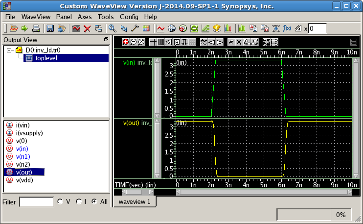
View the signal waveforms using Custom WaveView
In the upper "Output View" pane of the newly opened Custom WaveView window,
dounble-click on "D0:<cellname>.tr0" and then click on
"toplevel" in order to reveal signals in the lower "Output View" pane.
You can then either double-click on the required signals
(e.g. v(in) and v(out) )
or drag-and-drop them
into the right hand "waveview 1" pane.
The result should look like this:

Note that screen captures of waveform windows such as the one above should
never be used in a report because the black background obscures
the waves while the window border and buttons distract from the
information that you are trying to present.
Create a PDF copy of waveform display
First use the Preferences button on the Configuration tab to tell the system
that printers exist (we need to do this even if we don't print directly to
the printers).
    Configuration -> Preferences ...

      General
        Printer Devices:     [mono;colour              ]
        Unix Print Command:  [lp -d $printer $file     ]
      OK
Next use the Print button of the Waveform tab to create a black and white
PostScript (.ps) version of the waveforms:
    Waveform -> Print ...

      Print Setup
        Printer:                      [mono                     -]
        Paper Size:                   [A4   (210Wx297H mm)      -]
	[ ] Portrait  [ ] Color Print
      PostScript Output File
	[X] Print To File
        Output Path: [ <printfile>.ps                            ]
      Print
(select "colour" and "[X] Color Print" for colour printing).
Now convert the PostScript file to PDF using the ps2pdf unix command:
ps2pdf <printfile>.ps
Check that the file has been correctly generated using the evince document viewer:
evince <printfile>.pdf &
This PDF file can then be included in a report or printed directly
to the printer.
Print a copy of the waveform
print -d <printername> <printfile>.pdf
Measurements
Custom WaveView also includes a facility to take measurements from
the waveforms displayed via the Measure Tool which can be
invoked from the Utilities menu on the Waveform tab. This can be very useful
where .measure commands were not included in the spice file.
View the results of the .measure commands
Results are given in scientific notation with no units
(e.g. propagation_f = 2.249e-10 ) so you will need to
convert them into picoseconds or nanoseconds before
presenting them in any report (e.g.
Propagation delay
from in↑ to out↓ is 0.22ns).
Remember to perform "sanity checking" on your numerical
results. If the value provided by the .measure command
doesn't make sense when you try to match it to the waveforms
then you've probably mis-specified either the TRIGger or the
TARGet.
Additional Documentation


