
Integrated Circuit Engineering 2
The library includes standard cells designed for use in an SCMOS SUBMICRON process supporting 3 metal layers.
Metal1 will be used for power supply routing whereas Metal2 and Metal3 are used for two layer signal routing. Metal2 should run vertically while Metal3 runs horizontally.
Cells may be butted horizontally into rows. This will result in the automatic routing of power and ground between cells.
Rows may be butted vertically where the width of routing channels is sufficiently small. In this case every second row must be flipped such that power rails are adjacent to power rails and ground rails are adjacent to ground rails.
The library consists of the following leaf cells:
To ensure that the cells may be butted without causing design rule violations while enabling the routing of power and ground between adjacent cells in a row, the height of all cells and the arrangement of elements at the edge of the cells is tightly defined:

Note This explains why the power and ground rails are 1.5 lambda from the top and bottom of the cell. Some cell libraries will have this spacing set to zero to allow butting of power rails when cells are butted vertically. This is not permitted here since it leads to problems with wide metal (greater than 10 lambda). See rule 7.4 for details.
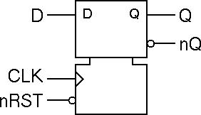
DFFR is an edge triggered D-Type flip flop with asynchronous reset.
The circuit is a standard six NAND gate implementation. Q takes on the value of D on the rising edge of the clock signal, CLK. The active low asynchronous reset signal is named nRST. An inverted output nQ is also supplied.
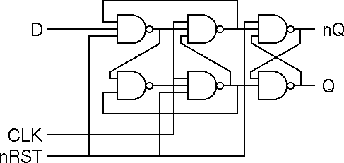
The schematic and symbol for this cell are found in the file: W:\TannerLibs\mAMIs05\MY_DESIGN.sdb with cell name BIM_DFFR.
Two altenative layouts for this cell are found in the file: W:\TannerLibs\mAMIs05\MY_DESIGN.tdb; BIM1_DFFR supports over cell routing while BIM2_DFFR supports routing channels which don't overlap with the cells.
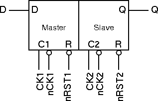
MSDR is a master slave D-Type flip flop with asynchronous reset.
The circuit is made up of two transparent latches driven by non-overlapping active high clocks, CK1 and CK2, and their complement signals, nCK1 and nCK2. The behaviour of the resulting circuit is the same as that of an edge triggered D-Type flip flop. Although the cell takes up less space than the corresponding edge triggered D-Type, the requirement for more complex clock generation and buffering may offset this benefit.
As with the edge triggered D-Type, an active low asynchronous reset has been included. For correct operation the two reset signals nRST1 and nRST2 should be connected together (thus master and slave latches are reset simultaneously).


The schematic and symbol for this cell are found in the file: W:\TannerLibs\mAMIs05\MY_DESIGN.sdb with cell name BIM_MSDR.
Two altenative layouts for this cell are found in the file: W:\TannerLibs\mAMIs05\MY_DESIGN.tdb; BIM1_MSDR supports over cell routing while BIM2_MSDR supports routing channels which don't overlap with the cells.

BUF is a non-inverting buffer with a nominal drive strength of 4.
The circuit is simply a pair of inverters with the transistors in the second ratioed such that they have four times the width of those in the first. The nominal drive strength is based on a unit inverter with Wn = 17 lambda and Wp = 34 lambda.
This circuit will be useful in driving high capacitance signals such as the output signals from your design and also as part of a clock tree for distribution of clock signals to D-Type elements.

The schematic and symbol for this cell are found in the file: W:\TannerLibs\mAMIs05\MY_DESIGN.sdb with cell name BIM_BUF.
Two altenative layouts for this cell are found in the file: W:\TannerLibs\mAMIs05\MY_DESIGN.tdb; BIM1_BUF supports over cell routing while BIM2_BUF supports routing channels which don't overlap with the cells.
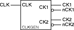
CLKGEN is a two phase clock generator suitable for use with the master slave D-Type MSDR.
The RS flip-flop consisting of two NOR gates creates the non-overlapping clocks. The two pairs of inverters serve to separate the clock phases further and to generate the inverted clock signals. The resulting waveforms are shown below.

Since each of the inverters generating one of the clock outputs has a nominal drive strength of only 1 the clock signals will need to be further buffered before driving more than a few MSDR circuits.
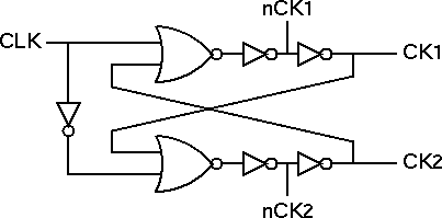
The schematic and symbol for this cell are found in the file: W:\TannerLibs\mAMIs05\MY_DESIGN.sdb with cell name BIM_CLKGEN.
Two altenative layouts for this cell are found in the file: W:\TannerLibs\mAMIs05\MY_DESIGN.tdb; BIM1_CLKGEN supports over cell routing while BIM2_CLKGEN supports routing channels which don't overlap with the cells.
Although it would be possible to ignore these provided cells and generate your own versions as required by your design, this approach is inefficient in manpower since you risk re-inventing the wheel.
Assuming that you choose to make use of the cells, you must decide which cells to use and how to get them to co-exist with your own cells:
You may use BIM1_ style layouts or BIM2_ style layouts but not both.
Your choice here should match the style used in your other cells. Thus if you use Metal2 or Metal3 for wiring within any of your leaf cells, you must use the BIM2_ style with i/o ports at the top and at the bottom of each cell for all leaf cells.
In general you should choose one or other of the D-Types rather than using both within a single design. This avoids the problem of skew between the single clock required by the edge triggered design and the multiple clocks required by the master slave design.
Where your new cells are taller than the given cells it is a relatively simple matter to stretch the given cells to meet your conventions. Where your new cells are shorter it may be possible to shrink the given cells although it is likely to be easier to stretch your new cells.
Whether or not you modify the given cells you should rename them with your team prefix (e.g. BIM1_BUF becomes ABC_BUF for Anne, Bob and Caroline's team ABC). This will avoid name conflicts when the designs from different teams are merged.
The cell library also includes a top level (or fabrication) cell named MY_DESIGN. This cell includes the location of all of the inputs and outputs to your design such that it can be incorporated into the final chip. You should rename this cell for use as your top level cell (e.g. ABC_DESIGN for team ABC). To avoid design rule violations, your final design must not overlap the edges of this cell.
Iain McNally
19-2-2003