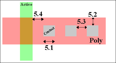
Simple Poly to Contact |
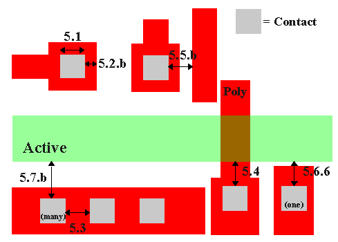
Alternative Contact to Poly |
On 0.50 micron process (and all finer feature size processes), it is required that all features on the insulator layers (CONTACT, VIA, VIA2) must be of the single standard size; there are no exceptions for pads (or logos, or anything else); large openings must be replaced by an array of standard sized openings. Contacts must be drawn orthogonal to the grid of the layout. Non-Manhattan contacts are not allowed.
If your design cannot tolerate 1.5 lambda contact overlap in 5.2, use the alternative rules which reduce the overlap but increase the spacing to surrounding features. Rules 5.1, 5.3, and 5.4, still apply and are unchanged.
Simple
|
Alternative
|
||||||||||||||||||||||||||||||||||||||||||||||||||||||||
|
|
||||||||||||||||||||||||||||||||||||||||||||||||||||||||

Simple Poly to Contact |

Alternative Contact to Poly |
If your design cannot handle the 1.5 lambda contact overlap in 6.2, use the alternative rules which reduce the overlap but increase the spacing to surrounding features. Rules 6.1, 6.3, and 6.4, still apply and are unchanged. Contacts must be drawn orthogonal to the grid of the layout. Non-Manhattan contacts are not allowed.
Simple
|
Alternative
|
|||||||||||||||||||||||||||||||||||||||||||||||||||||||||||||
|
|
|||||||||||||||||||||||||||||||||||||||||||||||||||||||||||||
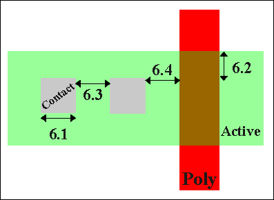
Simple Contact to Active |
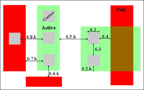
Alternative Contact to Active |