This year the task is to produce a novel general purpose microprocessor.
To demonstrate the usefulness of your design you will be asked to show that it can execute programs to perform the following tasks:
You may find that the resources for this project are rather less than those available to Intel in terms of:
For these reasons you should aim for the simplest design possible:
Your architecture should support a 16 bit wide datapath and a 216 word address space.
Your architecture should support subroutine call and return via a system stack. Your factorial program should use a recursive subroutine in order to demonstrate this facility. You should also support the use of the stack for parameter passing and local variable storage. A separate subroutine for multiplication (called by your factorial routine) should help to demonstrate these features.
Note that a dedicated stack pointer is not required in order to support this system stack. A simple RISC processor would simply use one of its general purpose registers as a stack pointer. Nor is it necessary to provide auto-increment or auto-decrement in order to support stack pull(push). A simple RISC processor would typically use different instructions for load(store) data and increment(decrement) stack pointer. In order to support local variable storage on the stack you will need to include a simple indexed addressing mode.
The stack should be a "Full Decending" type. This means that the stack pointer will point to the topmost element on the stack and the stack pointer is decremented in order to add a new element onto the top of the stack.
Your processor should employ no more than ten 16 bit registers, including the program counter (PC) and the instruction register (IR). Solutions with between four and ten registers are possible. This limit will help to keep processor sizes down and will encourage you to think carefully about the efficient use of the registers that you have.
Note that this is a limit not a target, thus it is perfectly acceptable for any team to submit a design with only four registers.
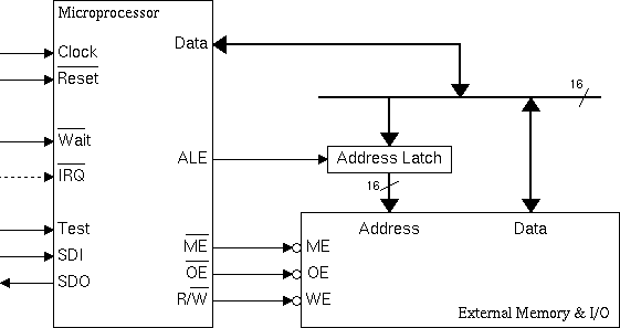
The system will consist of a central microprocessor (to be designed by you), connected via a single set of buses and some glue logic to external memory (e.g. ROM, RAM) and memmory mapped I/O.

There is no restriction on the area of your design. If your chip core plus pad wiring is smaller than 1410um by 1410um then it will fit into the default pad ring without modification. If your chip core is larger you can easily extend the pad ring with the addition of spacer cells between the pads.
Typically one design from each year's course is fabricated. In selecting the design to be fabricated, both the quality of the design and the efficiency of its implementation (i.e. it's area) will be considered.
As much as possible you are left to make your own decisions on the form of your design.
Hopefully the research phase of this project will give you a good starting point for attempting this design. Further research is likely to be required as your ideas develop. Although your design may have more in common with microprocessors of the late '70s than with modern RISC machines, the same principles of good design apply. Remember that you are not competing with the AMD Opteron, only with the designs put forward by other design teams.
All memory accesses take four cycles of the system clock
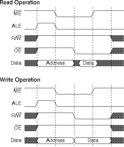
Note that it is this four cycle memory access that precludes the use of pipelining in your design. No benefit can be gained from pipelining here without the use of an on-chip memory cache which is not within the scope of this project.
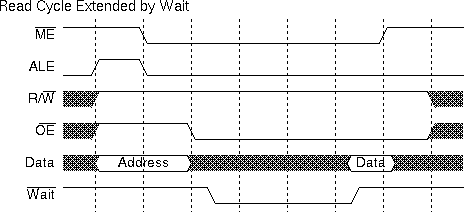
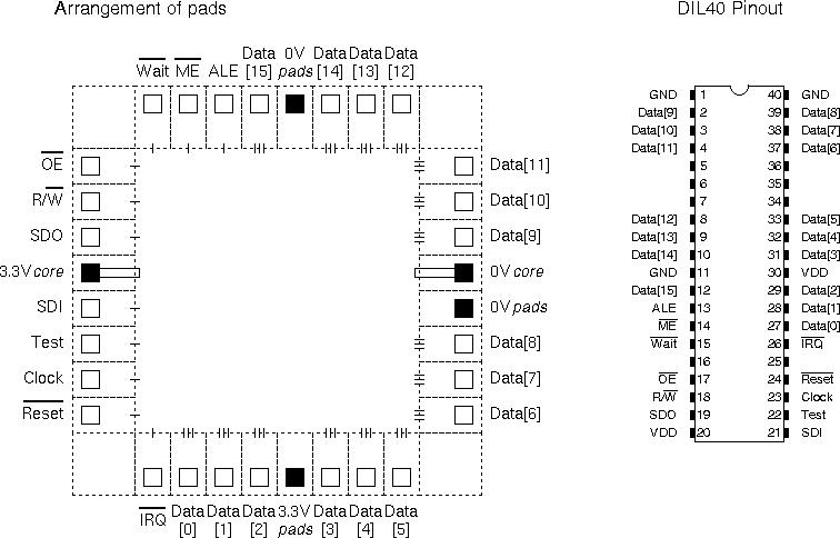
The nWait signal is used to lengthen the memory cycle when accessing slow peripherals. This input signal is normally high. It may be taken low by a slow peripheral during the Data Setup cycle. Should this occur, the microprocessor should remain in the Data Setup cycle until nWait becomes high again.
The nIRQ signal is an active low, level sensitive, interrupt request input. Support for this interrupt facility is an optional extra, allowing you to show off your talents.
Notes
Pad cells for this design will be taken from Alcatel Mietec's MTC35400 library for their 0.5um CMOS process. Alcatel provide us with empty abstract representations of these cells since the contents are considered company confidential. You will be provided with dummy versions of the cells which should simulate correctly using Magic and Verilog. To avoid design rule violations with the real pad cells you should keep routing wires one full design rule away from the edge of the pad cells except where connection is required.
The following types of pad are available:
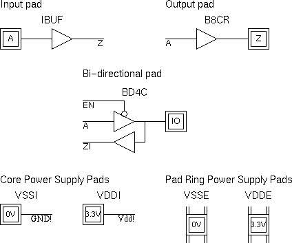
The following pads will exist on the finished chip:
These pads make no direct connection to the core circuit. This will reduce switching noise on the core power rails.
These pads include a non-inverting buffer and static protection circuit.
These pads include non-inverting pad drivers.
These pads include a tri-state non-inverting buffer (with inverted enable) on output and a non-inverting buffer on input. Three connections are made to the core of the cell in order to support a bi-directional pad. Although the pad connection is tri-state, the core connections are not, thus the ZI and A connections cannot be directly connected to the same internal bus.
Iain McNally
5-2-2008