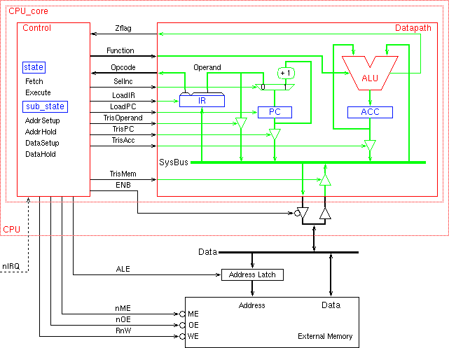
A very simple single bus processor has been designed using SystemVerilog Hardware Description Language.

The processor has a 16-bit data path and a 12-bit address space.
Each instruction is one word (16-bits) wide and consists of a 4-bit opcode and a 12-bit address operand:

The following instructions are supported:
Instruction	Opcode	Operation

  NOP		  0	No Operation
  JMP		  1	PC <= address
  JMPZ		  2	if (Z==1) then PC <= address
  JMPNZ		  3	if (Z==0) then PC <= address
  LDA		  4	Acc <= mem(address)
  ADD		  5	Acc <= Acc + mem(address)
  SUB		  6	Acc <= Acc - mem(address)
  AND		  7	Acc <= Acc & mem(address)
  OR		  8	Acc <= Acc | mem(address)
  NOT		  9	Acc <= ~Acc
  LSL		  10	Acc <= Acc << 1
  LSR		  11	Acc <= Acc >> 1
  STA		  15	mem(address) <= Acc
Note that this simple processor is too simple to meet the specification for the full custom design exercise because:
The SystemVerilog files are the same for all microprocessors designed for the full custom design exercise:
Top level module for the microprocessor
Memory and input/output modules
Bus interface module (includes address latch and detects bus timing violations) and address decoder
The system described is shown below with 2048 words of RAM (addresses 0-2047) and I/O including a bank of 16 switches (mapped at address 2048) and a bank of 16 LEDs (mapped at address 2049):
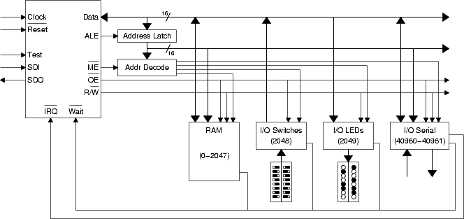
The
The arrangement of the components can be clearly seen in the architecture
diagram above.
Although the operation of the processor is simple and can easily be understood
from a study of the architecture diagram and the SystemVerilog code, it is worth
discussing the control unit in more detail:
All instructions complete in exactly two memory cycles (8 clock cycles).
The single bit state register is used to distinguish the first
(fetch) memory cycle from the second (execute) memory cycle.
The two bit sub_state register counts the four clock cycles
(address_setup, address_hold, data_setup &
data_hold) in each memory cycle.
Note that some instructions do not make full use of
the execute memory cycle since they do not need to make a second
memory access.
This mode of operation is chosen to simplify the control unit.
In the past many teams have experienced serious problems in the later
stages of the full custom design exercise due to complexities in their
control unit design.
Note also that the sub_state register follows a Gray code counting
sequence in order to avoid critical glitches on the memory timing signals;
ALE, nME, RnW & nOE.
In the past one design was fabricated with undetected problems with
its memory timing signals - the chip simulated but didn't work!
This year the simulation should flag any serious problems as timing
violations.
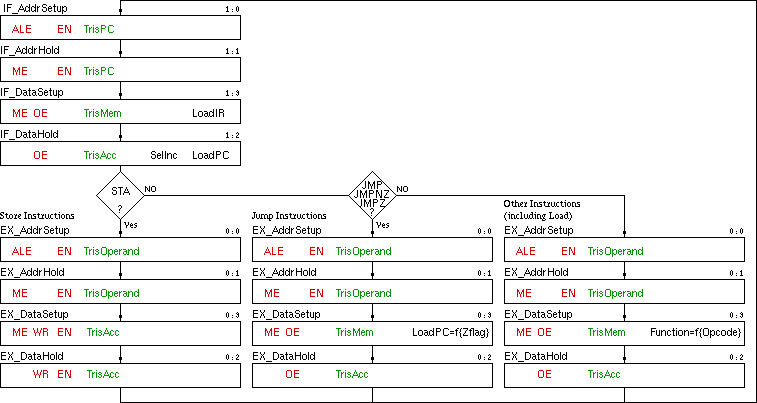
A simplified ASM chart for the control unit is shown below:
Notes
Signals are only shown when active.
TrisPC is shown active (i.e. =1) in IF_AddrSetup and IF_AddrHold
it is inactive (=0) in all other states.
To avoid confusion with active low signals, the chart shows
ME/OE/WR/EN, these may be considered as the non-inverted versions of the
active low signals nME/nOE/RnW/ENB. Thus where ME exists in the ASM chart,
we may assume that the virtual non-inverted signal ME is high and the
actual signal nME is low.
Exactly one Tris signal is active in each state since the Tris signals
determine which source drives the internal bus (SysBus).
Although the state machine has only 8 states, 16 are shown in
the ASM chart. This is a handy method to show the different behaviour
of the controller for each of the three different sorts of instruction
(Store, Jump, Other).
If you are bothered by this shorthand you may want to
draw the full ASM chart - very complex with conditional outputs, or
you may find it useful to think of the opcode stored in the instruction
register as a part of the state of the controller.
Most of the SystemVerilog modules above reference the
opcodes.svh package
file which defines the set of opcodes understood by the processor.
In addition there is an options.sv file
which is included by a number of the sytem modules and which defines marcos to control
simulation options:
When the simulation is invoked, the program is loaded from a
hex file into the ram.
By default the hex file loaded is:
The hex file can be generated in a number of ways; the simplest of
these is to use a SystemVerilog file which assembles the program using
pre-defined constants from the opcodes.svh
file and then outputs the result in the appropriate format:
The following assembly language instructions are coded in the example program
files:
Simple Program
        LDA    SWITCHES
        STA    varX
.loop   SUB   #1
        JMPZ  .done
        STA   varY
        ADD   varX
        STA   varX
        LDA   varY
        JMP   .loop
.done   LDA   varX
        STA   LEDS
        JMP   .end

.end    JMP   .end
This is approximately equivalent to the following `C' code:
X = SWITCHES;

Y = X;

while ( Y-1 != 0 )
   {
      Y = Y - 1;
      X = X + Y;
   }

LEDS = X;

while (TRUE) {}
Initialise your environment using the following command:
init_fcde_examplethis command will
Using the following command, you can investigate the operation of the processor:
./simulate
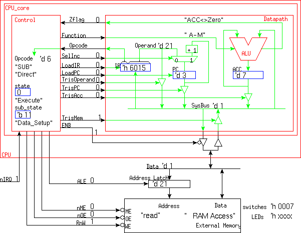
The following figure is a snapshot of the simulation:
The simulate script may also be called with options:
	./simulate +define+switch_value=8
	./simulate +define+special_stimulus
	./simulate +define+special_monitor
	./simulate +define+ram_access_time=2us
Note that the +define+special_monitor option has no effect since it is set as the default in the options.sv file.
To run an alternative program you can try:
./simulate example/new_prog.hexwhere example/new_prog.hex is a new hex format file that you have created.
or
./simulate example/new_program.svwhere example/new_program.sv is a new SystemVerilog program file that you have created. In this case the simulation will first assemble a new example/new_program.hex hex format file and then load the program from here into the ram for execution.
For your own HDL design, copy the example files to a new directory:
cp -r example mydesignThen edit the files in the new directory to reflect your design. You can simulate your design using:
./simulate mydesignSince you are likely to have more than one test program, you can specify the program file on the command line:
./simulate mydesign programs/myprog1.svNote that if you need to include options they should occur after the design directory and program file specification:
./simulate mydesign programs/myprog1.sv +define+switch_value=5
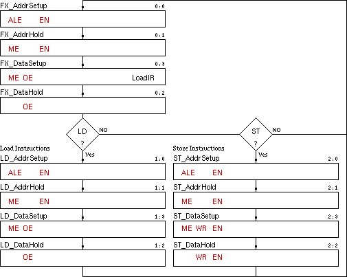
Below is a simple ASM chart suitable as a starting point for developing a RISC style controller where simple instructions are completed in 4 fetch and execute states while load and store instructions take a further 4 states to complete.
Iain McNally
27-2-2011