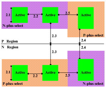
| Rule | Description | Lambda | ||
|---|---|---|---|---|
| SCMOS | SUBM | DEEP | ||
| 2.1 | Minimum width | 3 * | 3 * | 3 |
| 2.2 | Minimum spacing | 3 | 3 | 3 |
| 2.3 | Source/drain active to well edge | 5 | 6 | 6 |
| 2.4 | Substrate/well contact active to well edge | 3 | 3 | 3 |
| 2.5 | Minimum spacing between non-abutting active of different implant. Abutting active ("split-active") is illustrated under Select Layout Rules. | 4 | 4 | 4 |
| * Note: For analog and critical digital designs, MOSIS recommends the following minimum MOS channel widths (active under poly) for AMIS designs. Narrower devices, down to design rule minimum, will be functional, but their electrical characteristics will not scale, and their performance is not predictable from MOSIS SPICE parameters. | |||
| Process | Design Technology | Design Lambda (micrometers) | Minimum Width (lambda) |
| AMI_ABN | SCNA, SCNE | 0.80 | 5 |
| AMI_C5F/N | SCN3M, SCN3ME | 0.35 | 9 |
| AMI_C5F/N | SCN3M_SUBM, SCN3ME_SUBM | 0.30 | 10 |
