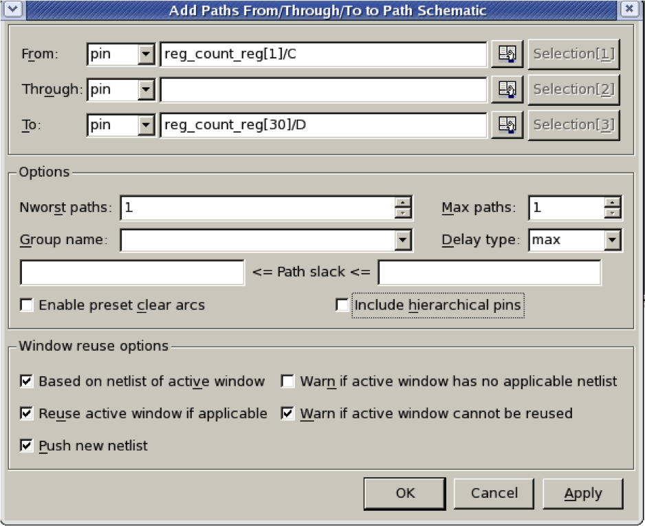
- In design vision: go to the Schematic menu and choose the option Add Paths From/To
- Fill in the starting point and end point of the critical path from the previous timing report
- Click ok
- Click ok again for the pop up window

After completing this unit, you should be able to:
For this lab you will need:
| Set up the library |
|---|
| Read in Design |
| Elaborate |
| Add Constraints |
| Map |
| Design Analysis |
| Timing Optimization |
| Design Write Out |
                               ams_demo
          ________________________|______________________
         |               |               |               |
    behavioural      constraints     gate_level      synthesis
dc_shell -gui
If you are logged into one of the Redhat 6 CAD servers (cadteaching, hart2 or hind2) the dc_shell command should already be in your search path and this command should run without any error messages (do not run any DC_Setup script).
If the .synopsys_dc.setup file is in the current working directory, the 0.35 um AMS technology library will automatically be loaded when dc_shell is invoked (there is no need to explicitly source any library setup file).
analyze -format sv "../behavioural/qmults.sv ../behavioural/wrap_qmults.sv"
Presto compilation completed successfully.
1
elaborate <modulename>
elaborate wrap_qmults
check_timing
Warning: the following end-points are not constrained for maximum delay.

End point
---------
complete
........
overflow
result_out[1]
result_out[0]
........
create_clock -period 20 -name master_clock [get_ports Clock]
set_max_area 0
This will instruct design compiler to use as little area as possible.
compile
To include a scan capable flip-flops, the command is:
compile -scan
This command may take a few minutes depending on the size of
the design.
This tells the which ports to use for the scan path control signals:
    set_dft_signal -view existing_dft -type ScanClock   -port <clock_port>  -timing {5 15}
    set_dft_signal -view existing_dft -type Reset       -port <nreset_port> -active_state 0

    set_dft_signal -view spec         -type ScanEnable  -port <test_port>   -active_state 1
    set_dft_signal -view spec         -type ScanDataIn  -port <sdi_port>
    set_dft_signal -view spec         -type ScanDataOut -port <sdo_port>
For the qmults example the following ports should work:
    set_dft_signal -view existing_dft -type ScanClock   -port Clock  -timing {5 15}
    set_dft_signal -view existing_dft -type Reset       -port nReset -active_state 0

    set_dft_signal -view spec         -type ScanEnable  -port Test   -active_state 1
    set_dft_signal -view spec         -type ScanDataIn  -port SDI
    set_dft_signal -view spec         -type ScanDataOut -port SDO
    create_test_protocol
    dft_drc
    set_scan_configuration -chain_count 1
    preview_dft
insert_dft
report_qor
This will provide information about the timing information, critical path slack,
critical path clock period, total design area and information about the CPU statistics.
report_power
This will provide information about dynamic and leakage power.
report_timing


    report_area > synth_area.rpt
    report_power > synth_power.rpt
    report_timing > synth_timing.rpt
It is important to ensure that the naming styles of variable in the design are appropriatefor the target output language we are using (Verilog in this case). We can firstly see what names need changing:
report_names -rules verilog
If we are happy with the proposed new names we can perform the name changing process:
change_names -rules verilog -hierarchy -verbose
This is the final step in the synthesis flow, it allows the designer to transfer the synthesised circuit to the next stage of the design flow. This can be done as follows:
write -f verilog -hierarchy -output "../gate_level/qmults_syn.v"
write_sdc design.sdc
write -f verilog -hierarchy -output "../gate_level/qmults_syn.v"
write_sdf design.sdf
    analyze -format verilog  "../behavioural/qmults.sv ../behavioural/wrap_qmults.sv"

    elaborate wrap_qmults
    create_clock –name master_clock  -period 20 [get_ports Clock]
    compile
    report_area > synth_area.rpt
    report_power > synth_power.rpt
    change_names -rules verilog -hierarchy -verbose

    write -f verilog -hierarchy -output "../gate_level/qmults_syn.v"

    write_sdc design.sdc
    write_sdf design.sdf

    exit
There are many ways in which a designer can tweak the design at the synthesis stage to obtain the target performance :
compile -map_effort high
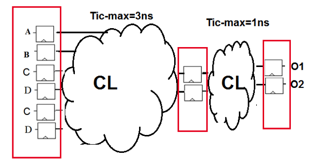
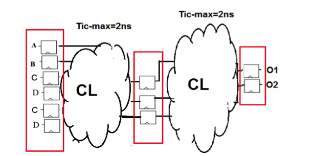
balance_registers
 |
=> |  |
 |
=> | 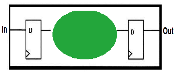 |
    current_design <modulename>
    ungroup -all -flatten
    compile -map_effort high -incremental_mapping
However, this option is not suitable for usage if the hierarchical design is large.
Too huge a design will take up considerable computing resources
(for example, a long time to compile).
set_implementation <implementation_type> <cell_list>
set_implementation cla A1
| Implementation type | Description |
|---|---|
| rpl | Ripple carry |
| cla | Carry look ahead |
| clf | Fast carry look ahead |
| sim | Simulation model |
report_resources
remove_attribute [get_cells *] implementation
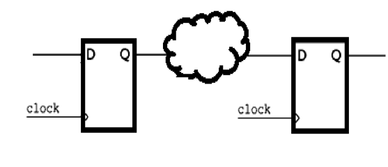 |
=> | 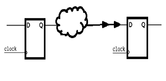 |
    set_fix_hold   <clock_name>
    compile –map_effort high -incremental_mapping
set_fix_hold clk1
remove_attribute [get_clocks clk1] fix_hold