Overview of a Simple RISC-V SoC
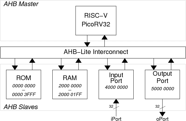
A very simple RISC-V System on Chip has been designed:

- ROM
16K bytes for program memory - RAM
512 bytes for data memory (including stack) - Input Port
Occupying one 32-bit memory location - Output Port
Occupying one 32-bit memory location
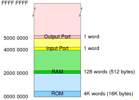
Memory Map
-
The memory map is sparsely populated with the unused areas being filled with secondary images
of the real slave devices:

The secondary images are an artefact of the partial address decoding which only uses the top 4 address bits (HADDR[31:28]) in order to decide which slave is being accessed.
Files
In order to build the RISC-V SoC, we need SystemVerilog files to model the hardware plus 'C' program files and other support files to build the software. Further files are required to support simulation:
- Hardware
- Software
- Simulation
Preparation
- Create a new directory for the lab (e.g. ~/design/system_on_chip/example_riscv_asic_simplified)
and change to the new directory:
mkdir -p ~/design/system_on_chip/example_riscv_asic_simplified cd ~/design/system_on_chip/example_riscv_asic_simplified - Copy the design files:
init_riscv_soc_asic_simplified_example -here
Compile C Program
- In the software sub-directory, the
makefile and the
soc.ld linker script
are used to compile the main C language file:
main.c,
and the support files:
start.s and
crt.c.
Running the appropriate make commands in the software directory:
    cd software
    make clean
    make code.vmem
should create a Verilog hex format file named "code.hex" which could be used in simulation but not in ASIC synthesis and a "code.vmem" version of the same hex data which is better suited to ASIC synthesis. - Open the "code.hex" and "code.vmem" files in a text editor to check that they have been created.
- Run an additional make command to create a dissassembly listing of the program:
make code.lstExamining the "code.lst" file in a text editor can be very helpful when trying to debug a system-on-chip design in simulation.Note that you can generate "code.hex", "code.vmem" and "code.lst" files at the same time using the following make command:
make all
Simulate RISC-V SoC
- In the main directory (~/design/system_on_chip/example), a
simulate script exists to
simplify the task of running the simulation:
    cd ..
    ./simulate &
(The xmverilog command to run the simulation is:
    xmverilog +gui +access+r \
              +tcl+testbench/soc.tcl \
              -y behavioural +libext+.sv \
              +define+prog_file_vmem=software/code.vmem \
              testbench/soc_stim.sv
but it's easier to use the simulate script) - Consult the HADDR and HSEL_... signals in the waveform window and satisfy yourself that the correct active HSEL_... signal is being selected based on any particular address value. (Identify at least one address for each of the HSEL_... signals and confirm that it is in the correct range)
- Look at the Console output and the main.c program. Can you explain the sequence of "oPort" values that you see in simulator console?
- Add the contents of the RAM to a memory viewer window and work out how much of the RAM is in use with this program. (You will have to 'rewind' and re-run the simulation in order to see
the contents of the RAM).
You are looking for three regions:
- Global data (lower memory addresses)
- Unused memory (a region of XXXXXXXX locations between the global data and the stack)
- Stack data (higher memory addresses)
Note that because the stack grows downwards, the higher memory addresses are used before the lower ones.
Although the stack may be sparsely used (there are likely to be unused XXXXXXXX locations in the stack), it should still be possible to identify the larger area of unused memory between the globals and the stack.
Create a custom interface
The key to system-on-chip design is the creation of custom slave hardware.
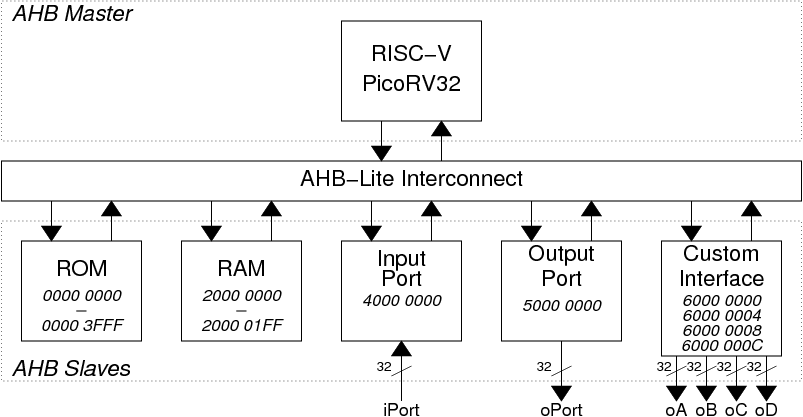
A modified ARM System on Chip including a simple custom interface is to be designed:

- Create the custom interface
The file name for the interface should be ahb_custom_interface.sv and it should be placed in the existing behavioural/ directory.
A template for the custom interface can be found here: ahb_custom_interface.sv
You will need to take the template and fill in the code where it is missing. You can base the code that you enter on the code from the output port module: ahb_output_port.sv. Since the custom interface supports more than one address, you will need to add code to generate a word_address signal during the address phase. An example of this sort of code can be found in this example module: ahb_switches.sv
- Create a new SoC top-level module
The file name for the top-level module should be soc_custom.sv and it should be placed in the existing behavioural/ directory.
You can base the new module on the existing SoC module code: soc.sv.
Changes that you should make are:
- The module name needs to be changed to soc_custom
- In addtion to the existing oPort output port, you will need to create four new output ports: oA, oB, oC and oD.
- In the "Per-Slave AHB Signals" section, you will need to add the following wires for the custom slave: HSEL_CUSTOM, HRDATA_CUSTOM and HREADYOUT_CUSTOM.
- In the "AHB interconnect" section, you will need to add the the same wires
(HSEL_CUSTOM, HRDATA_CUSTOM and HREADYOUT_CUSTOM)
into the signal buses to be connected to to the "AHB_interconnect" module.
Since this new slave will have the highest base address, the new signals will need to be added at the left (most significant) end of each signal bus concatenation. Thus:
{HSEL_OPORT,HSEL_IPORT, ...will become:{HSEL_CUSTOM,HSEL_OPORT,HSEL_IPORT, ... - Under the ahb_output_port module instance you should add a module instance for the new interface, ahb_custom_interface.
- Update the memory map in the interconnect module: ahb_interconnect.sv
- At the top of this file you will need to change the num_slaves parameter to match the number of bus slaves in the new system (5).
- In the "Decoder" part of the file add a condition "if ( HADDR < 32'h6000_0000 )" for the "HSEL_SIGNALS = 1 << 3;" option and a new default/else option "HSEL_SIGNALS = 1 << 4;".
- Simulate the complete design
The testbench/ directory already includes a soc_custom_stim.sv testbench file to test the new system. The command to use is:
./simulate testbench/soc_custom_stim.sv &If all goes well, the behaviour of the new system will match that of the old one since the the 'C' program is unchanged (there are no memory accesses for the custom slave).
- Modify the 'C' program
Now modify the 'C' program to access the other registers in the custom interface.
Changes that you should make are:
- Add the following 'C' code to enable the registers within the custom
interface to be accessed:
// Define the raw base address value for the custom interface

#define AHB_CUSTOM_BASE                         0x60000000

// Define a pointer with correct type for access to 32-bit registers
//
// The the four registers in the interface can then be accessed as:
//    CUSTOM_REGS[0]
//    CUSTOM_REGS[1]
//    CUSTOM_REGS[2]
//    CUSTOM_REGS[3]

volatile uint32_t* CUSTOM_REGS = (volatile uint32_t*) AHB_CUSTOM_BASE;
- Add 'C' code at the beginning of the main function to set oA=63, oB=56, oC=121 and oD=118.
- Add 'C' code within the while(1){...} loop to set oC equal to read_switches().
- Add 'C' code within the while(1){...} loop to set oD equal to oC + 1.
After each change you should recompile the code then re-run the simulation and check that the new behaviour is as you expect.
- Add the following 'C' code to enable the registers within the custom
interface to be accessed:
Create an AHB slave with side effects
Most custom slaves combine addressable registers (such as the 4 registers in the example above) and side effects (where reading or writing a register causes something else to happen.
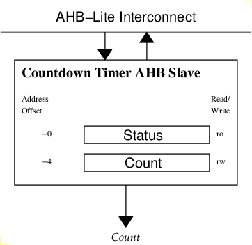
The following figure shows a countdown timer slave with two addressable registers:

- Writing to the Count register should have the side effect of starting the countdown.
Exactly one millisecond after the register is written, the value in the Count register will
be decemented by 1. This will continue every millisecond until the Count value reaches zero.
- The Status register is a read-only register. It will contain the value 1 while the countdown is taking place and 0 when the countdown is complete. By checking the Status register before writing to the Count register it is possible to ensure that one countdown is complete before the next countdown is started.
Using the same techniques as used for the custom interface above, add the timer slave to your design and write a program which runs a countdown for 50 milliseconds, then a second countdown for 100 milliseconds after which it should start again.
Note that you may find it easier to replace the custom interface with the new timer slave rather than adding the timer slave to the existing setup since the ahb_interconnect module does not need updating if the total number of slaves remains the same.
Having completed this lab walkthrough, you should have a basic understanding of SoC design including an ability to build a simple custom interface and write a 'C' program to access the interface.
At this stage you can experiment with other changes to the system but you should try to make only small changes between simulations to increase the chances of being able to debug the system.
Iain McNally
28-1-2025