

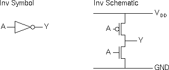
For hierarchy we need clearly defined symbols for each schematic.
- Top level symbol and schematic

- Symbols and schematics for sub-circuits
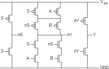
The same multiplexor may be shown as a flat schematic.
Circuit schematic diagrams offer a way for you to present your circuit designs to others. It is very important that the information you present is clear and unambiguous.
This document will show you some examples of simple schematics and then discuss the key issues involved in producing good schematics for yourself. This document cannot tell you exactly how to design all of your schematics; you will have to use your own judgement in each individidual case to give the best presentation of your circuit.
Although written for digital IC design, most of the principles apply equally to other circuit schematics.


For hierarchy we need clearly defined symbols for each schematic.


The same multiplexor may be shown as a flat schematic.

Ensure that your circuit schematics are easy to read.
Many students take the view that if they are using a schematic capture tool, then the schematic is finished when an automatic schematic check succeeds or when they are able to simulate an extracted netlist. Unfortunately this is far from sufficient to ensure readability. If you intend including schematics in a future report, it is a good idea to start by assuming that all schematics that you create with a schematic capture tool should be as human readable as possible.
It is very easy to over complicate a schematic with too many components, with components in the wrong place or with spaghetti wiring.
Careful use of hierarchy allows for the number of components on each schematic to be reduced, leaving the design simpler to follow.
At higher levels in the hierarchy we can also simplify wiring by:
In gate level schematics we omit power and ground connections.
In some block schematics global clock and reset signals may also be omitted.
Note that the use of three terminal transistor symbols in digital schematics is an example of this sort of simplification. Substrate connections can be omitted since all NMOS substrate connections are to GND and all PMOS substrate connections are to VDD.
Note that you can use hierarchy in your schematics even if your layouts are designed flat (without hierarchy).
Occasionally you will do better to consider a flat schematic such as the following example of euler path investigation in a six NAND gate D-Type (Euler paths that span multiple NANDs cannot be seen in a hierarchical schematic):

On a schematic, any two wires with the same label are connected. Careful use of this facility can avoid the sort of spaghetti wiring shown below:
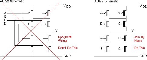
Note here that the extra wiring actually makes it harder to see which input is connected to which transistor.
Left -> Right
Ensure that there is a clear signal flow from left to right.
Circuit inputs should be on the left while outputs should be on the right. Similarly symbols should normally have inputs on the left and outputs on the right. Where these conventions are not followed it becomes necessary to include arrows on wires to indicate the direction of signal flow:

Here arrows are not added where signal flow is left to right to avoid cluttering the schematic.
Where we have bidirectional signals (such as the DataBus signal in the schematic below) we need to include arrows to indicate bidirectional and/or unidirectional ports for the blocks:
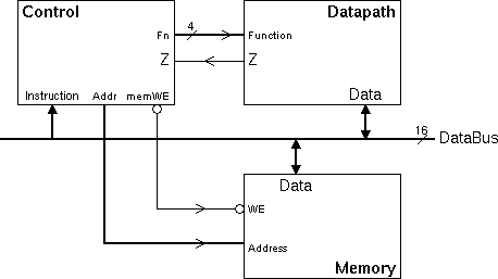
Note that in this diagram, it is not possible to show a distinct left to right signal flow. Here the addition of arrows on all wires helps to clarify the flow.
Wiring should be arranged to reduce the number of crossovers. Be careful with your presentation of connections and crossovers:

Although some CAD tools permit the use of a "solder dot" to connect wires which would otherwise appear to cross, this is considered poor style since small solder dots are often lost during photocopying while large solder dots obscure the picture. You should not use solder dots in your schematics. Similarly bridges complicate a schematic unnecessarily and should not be used.
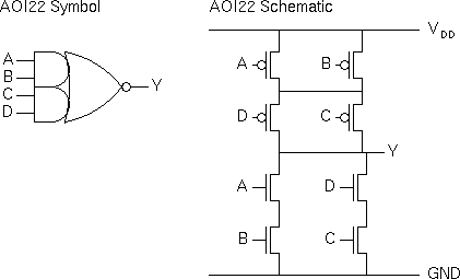
Many students have problems distinguishing schematics from symbols where compound gates are involved.

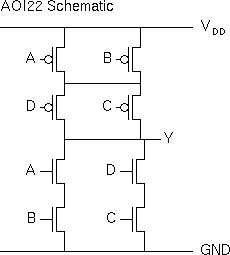
(A) Shows the symbol for a compound gate which is implemented using 8 transistors:
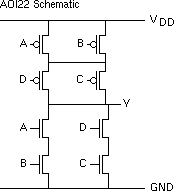
(B) Shows a circuit schematic. For the implementation of this we must consider sub-circuit schematics for the AND and NOR symbols. Here we have 16 transistors (6 for each AND gate and 4 for the NOR gate).

Since compound gates are only found on ICs, compound gate symbols are not found in schematic capture packages not customized for IC design (although many packages allow you to create your own symbols).
Iain McNally
1-12-2003